Revealing High-Speed Material Properties for Tomorrow's Digital Infrastructure
D-ITET researchers have taken a significant step towards advancing next-generation communication technologies by unveiling the electro-optical properties of lithium niobate (LN) and barium titanate (BTO). Their findings, published in Nature Materials, provide the first comprehensive characterization of these materials across an unprecedented frequency range.
Advancing Photonic Integrated Circuits
A team of researchers from the Institute of Electromagnetic Fields (IEF) has addressed a critical knowledge gap towards the development of photonic integrated circuits. The results were published in the most recent issue of Nature Materials. The study, entitled "Barium titanate and lithium niobate permittivity and Pockels coefficients from megahertz to sub-terahertz frequencies", provides the first comprehensive characterization of two essential materials used in photonic integrated circuits across an unprecedented frequency range.
The research focuses on the key materials lithium niobate (LN) and barium titanate (BTO) that exhibit the Pockels effect, which allows a material’s interaction with light waves to be tuned using electrical signals. The effect is widely used in photonic circuits for applications like fiber communications where light rather than electricity carries digital information.
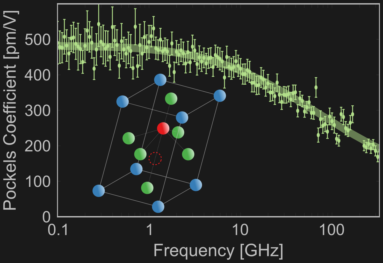
Comprehensive Characterization Across a Wide Frequency Spectrum
"Our work represents the first comprehensive characterization of these materials across this wide frequency spectrum", says Dr. Daniel Chelladurai, the study's lead author. "We were particularly surprised by BTO's strong frequency dependence, which contrasts sharply with the stable response observed in lithium niobate. Despite this variation, we demonstrated that BTO offers remarkable electro-optic performance up to the highest frequencies."
To extract the material properties, the researchers introduced specialized waveguide structures along with a measurement technique that allowed them to directly characterize these materials in actual devices. This approach provides a unique insight into material behavior under real operating conditions.
Implications for the Development of Photonic Integrated Circuits
Professor Juerg Leuthold, who leads the research group at the Institute of Electromagnetic Fields (IEF), emphasized the broader implications: "Photonic integrated circuits represent the next frontier in information processing technology. By understanding how these materials behave across such a wide frequency range, we've created a foundation for designing devices that can operate at speeds previously considered challenging. Our measurement approach also provides a standardized method for evaluating new materials that might soon emerge."
The implications of this work extend to numerous emerging technologies, including:
• High-speed optical communications beyond 100 GHz
• Quantum networks requiring efficient microwave-to-optical conversion
• Programmable photonic circuits
• Reconfigurable metasurfaces for augmented and virtual reality
Laying the Groundwork for Future Electro-Optic Materials
The research establishes both a comprehensive data set for current materials and a methodological framework for characterizing future electro-optic materials. The team at IEF hopes the work will accelerate the development of next-generation photonic integrated circuits that can operate at unprecedented speeds.
The complete article is available online: external page Nature Materials.